EN
EN
 AR
AR
 BG
BG
 HR
HR
 CS
CS
 DA
DA
 NL
NL
 FI
FI
 FR
FR
 DE
DE
 EL
EL
 HI
HI
 IT
IT
 JA
JA
 KO
KO
 PL
PL
 PT
PT
 RU
RU
 ES
ES
 SV
SV
 TL
TL
 IW
IW
 ID
ID
 LV
LV
 SR
SR
 UK
UK
 VI
VI
 GL
GL
 HU
HU
 TH
TH
 TR
TR
 AF
AF
 MS
MS
 SW
SW
 GA
GA
 CY
CY
 IS
IS
 BN
BN
 BS
BS
 NE
NE

Where to Use Straight-Through Pogo Pin in PCB Layouts
The straight-through pogo pin has emerged as a critical component in modern PCB design, offering engineers a reliable solution for establishing electrical connections in space-constrained applications. Unlike traditional right-angle connectors, these specialized spring-loaded pins provide a direct vertical connection path that maintains signal integrity while accommodating mechanical tolerances. As electronic devices continue to shrink in size while demanding higher performance, understanding the optimal placement and application of straight-through pogo pins becomes essential for successful PCB layout design.
Fundamental Design Principles for Pogo Pin Integration
Electrical Considerations in PCB Layout
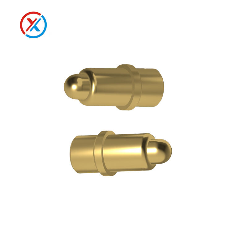
When implementing straight-through pogo pin configurations, electrical performance must remain the primary design consideration. The direct connection path minimizes signal degradation while maintaining consistent impedance characteristics throughout the transmission line. Engineers must carefully calculate trace routing to ensure proper impedance matching, particularly in high-frequency applications where signal integrity becomes critical. The spring mechanism within each pin provides reliable electrical contact while accommodating manufacturing tolerances that might otherwise compromise connection reliability.
Signal routing around pogo pin locations requires strategic planning to minimize electromagnetic interference and crosstalk between adjacent circuits. The metallic construction of these connectors can create unwanted coupling effects if not properly isolated through ground plane management and appropriate spacing techniques. Designers should implement guard traces and maintain adequate clearance distances to preserve signal quality while maximizing the benefits of the straight-through configuration.
Mechanical Integration Requirements
The mechanical aspects of straight-through pogo pin implementation demand precise attention to mounting hole dimensions and PCB thickness considerations. These connectors rely on controlled compression forces to maintain electrical contact, requiring careful calculation of engagement distances and spring travel limits. The PCB substrate must provide sufficient mechanical support to withstand repeated insertion and extraction cycles without compromising structural integrity or electrical performance.
Proper mechanical design includes consideration of mating connector alignment and the potential for angular misalignment during connection processes. The spring-loaded mechanism compensates for minor positioning variations, but excessive misalignment can lead to premature wear or connection failure. Engineers should specify appropriate tolerances and include alignment features in their mechanical design to ensure reliable long-term operation.
Strategic Placement in High-Density Layouts
Space Optimization Techniques
Modern electronic devices demand maximum functionality within increasingly compact form factors, making efficient space utilization critical for successful PCB design. The straight-through pogo pin configuration offers significant advantages in high-density layouts by eliminating the lateral space requirements associated with traditional connector types. This vertical connection approach allows designers to position multiple connection points in close proximity without compromising electrical performance or mechanical reliability.
Component placement strategies should account for the thermal characteristics of pogo pin connections, particularly in applications where power transmission occurs through these interfaces. Heat generation from electrical resistance can affect both the connector performance and surrounding components, requiring careful thermal management through copper pour techniques and component spacing optimization. The direct connection path inherent in straight-through designs typically reduces resistance compared to alternative connector configurations, contributing to improved thermal performance.
Multi-Layer PCB Applications
Multi-layer PCB designs benefit significantly from the implementation of straight-through pogo pin connections, particularly when establishing inter-board communication paths or power distribution networks. The vertical connection pathway allows signals to traverse multiple layers efficiently while maintaining controlled impedance characteristics throughout the connection. This approach proves especially valuable in stackable PCB configurations where multiple boards must communicate through reliable electrical interfaces.
Layer stack-up considerations become critical when implementing these connectors in complex multi-layer designs. The via structures required to route signals to pogo pin connection points must be carefully planned to avoid creating unwanted stub effects or impedance discontinuities. Proper via placement and sizing ensure that signal integrity remains intact throughout the entire transmission path, from the source circuit through the pogo pin connection to the destination.
Application-Specific Implementation Strategies
Test and Programming Interfaces
Test fixture applications represent one of the most common uses for straight-through pogo pin configurations, where temporary connections must be established quickly and reliably. The spring-loaded mechanism allows test equipment to make consistent electrical contact with PCB test points without requiring permanent soldered connections. This approach significantly reduces test setup time while providing the electrical performance necessary for accurate measurements and programming operations.
Programming interface designs benefit from the repeatable connection characteristics of these connectors, particularly in production environments where thousands of devices require firmware installation. The straight-through configuration ensures consistent contact pressure and electrical performance across multiple programming cycles, reducing the likelihood of programming failures due to poor electrical connections. Proper PCB layout includes adequate spacing around programming points to accommodate test fixture alignment and operator access.
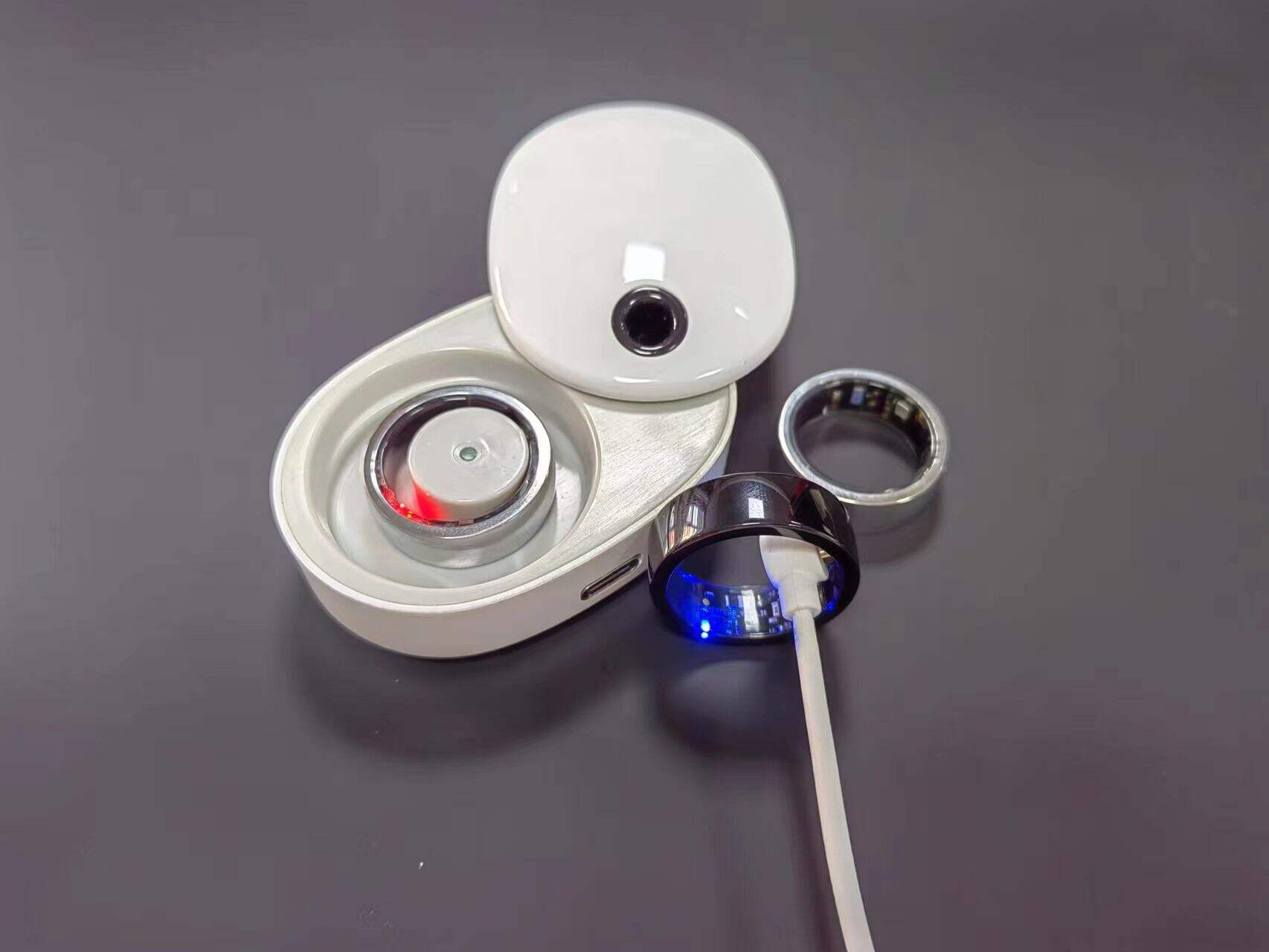
Battery and Power Connections
Power transmission applications place unique demands on pogo pin connections, requiring careful consideration of current carrying capacity and contact resistance characteristics. The straight-through design minimizes resistance in the connection path, making it ideal for battery charging applications where efficiency directly impacts charging time and energy consumption. The spring mechanism maintains consistent contact pressure even as battery cells expand and contract with temperature variations.
Charging circuit layouts must account for the thermal effects of power transmission through pogo pin connections, implementing appropriate copper pour techniques to distribute heat effectively. The gold plating commonly used on these connectors provides excellent corrosion resistance and low contact resistance, essential characteristics for reliable power transmission over extended operating periods. Proper thermal management prevents overheating that could degrade connector performance or damage surrounding components.
Signal Integrity and Performance Optimization
High-Frequency Design Considerations
High-frequency applications demand careful attention to the electromagnetic characteristics of straight-through pogo pin connections, where even minor impedance discontinuities can significantly impact signal quality. The connector geometry and PCB layout must work together to maintain controlled impedance throughout the entire signal path, including the transition regions where traces connect to the pogo pin interface. Proper design techniques include impedance matching networks and ground plane continuity management.
Signal routing strategies should minimize the length of high-frequency traces connected to pogo pin interfaces, reducing the potential for signal degradation and electromagnetic interference. The spring mechanism inherent in these connectors can introduce variable inductance effects that must be accounted for in high-speed designs. Careful connector selection and PCB layout optimization help minimize these effects while maintaining the mechanical advantages of the spring-loaded connection.
Grounding and Shielding Techniques
Effective grounding strategies become critical when implementing straight-through pogo pin connections in sensitive analog or high-speed digital circuits. The connector mounting structure should provide a low-impedance path to the PCB ground plane, minimizing ground bounce effects that could compromise signal integrity. Proper via placement and ground plane design ensure that return currents have direct paths back to their sources without creating unwanted loop areas.
Shielding considerations may require additional PCB design features to isolate sensitive circuits from the electromagnetic effects of pogo pin connections. Guard rings and ground fills around connector areas help contain electromagnetic fields while providing improved signal isolation between adjacent circuits. The metallic construction of these connectors can provide some inherent shielding benefits when properly connected to the PCB ground system.
Manufacturing and Assembly Considerations
PCB Fabrication Requirements
PCB fabrication for straight-through pogo pin applications requires precise control of hole dimensions and plating thickness to ensure proper connector fit and electrical performance. The mounting holes must accommodate the connector barrel while providing sufficient plating coverage for reliable electrical connection. Drill tolerances become critical, as oversized holes can lead to poor electrical contact while undersized holes may prevent proper connector installation.
Surface finish selection plays a crucial role in the long-term reliability of pogo pin connections, with hard gold or selective plating often preferred for contact areas that will experience repeated connection cycles. The PCB substrate material must provide adequate mechanical support for the connector while maintaining dimensional stability across temperature variations. Proper material selection ensures that the mounting structure remains secure throughout the product lifecycle.
Quality Control and Testing
Quality control procedures for PCBs incorporating straight-through pogo pin connections must verify both electrical and mechanical performance characteristics. Electrical testing should confirm proper continuity and resistance values while identifying any potential intermittent connection issues that could affect long-term reliability. Mechanical testing verifies proper connector engagement and spring compression characteristics to ensure consistent performance across multiple connection cycles.
In-circuit testing strategies should account for the removable nature of pogo pin connections, implementing test procedures that verify circuit functionality both with and without external connections. This approach helps identify potential issues with connector mounting or PCB layout that might not be apparent during initial electrical testing. Proper test fixture design ensures repeatable test results while minimizing wear on the pogo pin connections during production testing.
FAQ
What are the key advantages of using straight-through pogo pins in PCB layouts?
Straight-through pogo pins offer several significant advantages including space efficiency due to their vertical connection profile, reliable spring-loaded contact mechanism that accommodates manufacturing tolerances, excellent signal integrity through direct connection paths, and reduced electromagnetic interference compared to traditional connectors. They also provide consistent electrical performance across multiple connection cycles and can handle both power and signal transmission effectively in compact designs.
How do I determine the proper spacing between straight-through pogo pins?
Proper spacing depends on several factors including electrical requirements, mechanical constraints, and thermal considerations. For signal applications, maintain at least 2-3 times the pin diameter between adjacent pins to minimize crosstalk. Power applications may require greater spacing to manage thermal effects. Consider the mating connector requirements, manufacturing tolerances, and any shielding or isolation needs when determining final spacing dimensions.
What PCB thickness considerations apply to straight-through pogo pin implementations?
PCB thickness must accommodate the connector barrel length while ensuring adequate mechanical support. Standard implementations typically work with PCB thicknesses ranging from 0.8mm to 3.2mm, but specific connector models may have different requirements. The PCB must be thick enough to provide mechanical stability during connection cycles while not exceeding the connector's maximum engagement depth specifications.
How do straight-through pogo pins affect signal integrity in high-speed applications?
In high-speed applications, straight-through pogo pins can actually improve signal integrity compared to traditional connectors due to their shorter connection path and reduced impedance discontinuities. However, careful attention must be paid to impedance matching, via design, and ground plane continuity. The spring mechanism can introduce variable inductance effects, so proper connector selection and PCB layout optimization are essential for maintaining signal quality at high frequencies.
Hot News
-
Challenges for Pogo pin manufacturers in the AI era
2023-12-14
-
Teach you how to understand Pogo pin spline structure
2023-12-14
-
What products can Pogo pin be used in?
2023-12-14
-
How to choose Pogo pin connector
2023-12-14